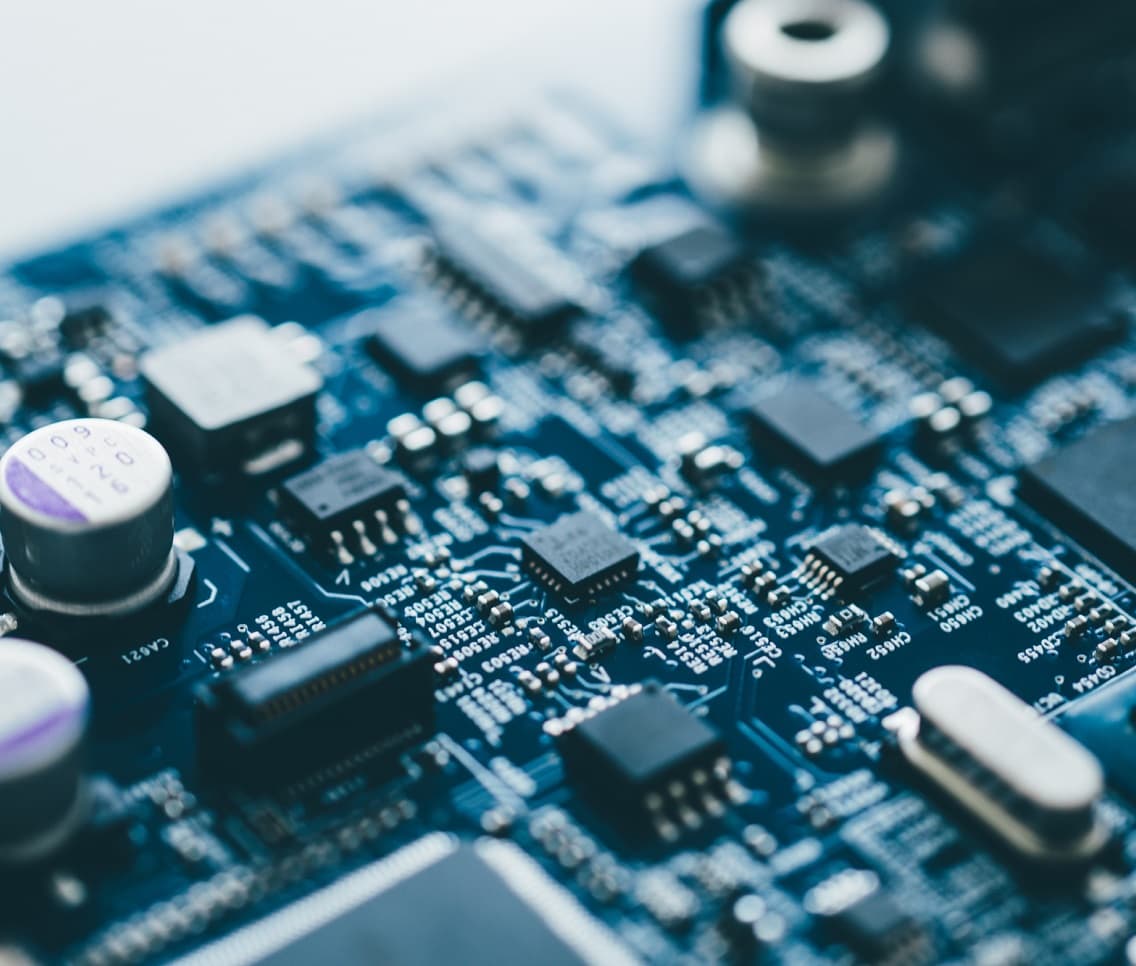
PCB Assembly & SMT
Complete solutions from simple
devices to critical computing
applications

THE PARPRO PCBA PRODUCTION ADVANTAGE
Advanced Manufacturing for Next-Generation PCBA
With over 20 years of experience in Printed Circuit Board (PCB) Assembly, PARPRO has grown to become a one-stop electronic contract manufacturer for complete PCBA manufacturing & printed circuit board assembly services. With our specialized design for manufacturability (DFM) and our relentless dedication to in-process quality control, leading OEMs rely on PARPRO for custom PCB assembly/testing of their most progressive and reliable embedded computing products.
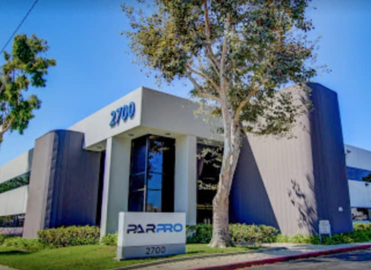
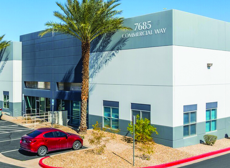
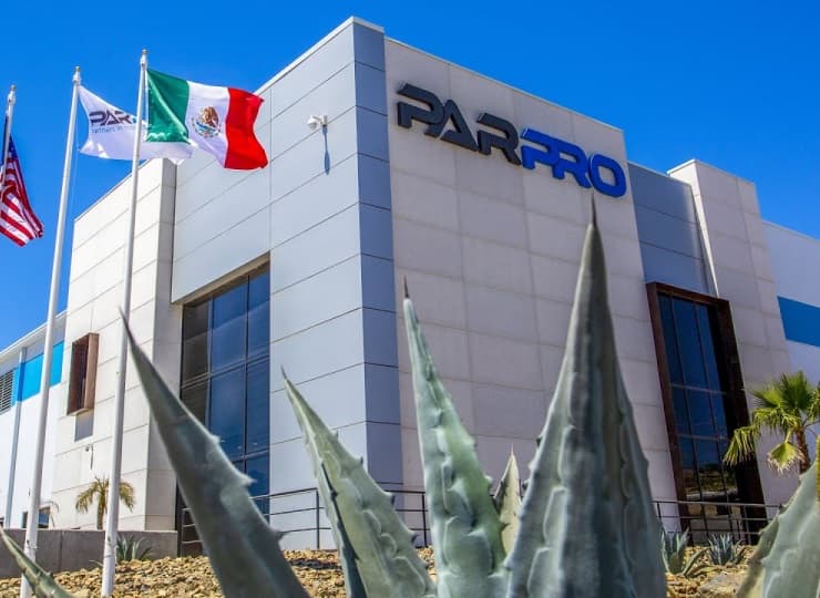
With North American headquarters in Southern California, we have PCBA manufacturing facilities in both USA and Mexico to provide the most affordable prices for the procurement of high-quality electronic components, making us an ideal supplier to both domestic and international customers/manufacturers.


PCB ASSEMBLY SERVICES
From Prototyping, Low Volume High Mix to Mid-Volume Manufacturing
Using the most advanced equipment, highly skilled and experienced personnel, and efficient processes, PARPRO undertakes all its PCBA manufacturing processes and operations in accordance with ISO 9001 / 13485 /14000 standards and compliance with the IPC-A-600 and IPC-A-610 Acceptability of Printed Boards Standards. In addition, PARPRO offers serialization, component/lot traceability and reverse logistics, along with a full range of PCBA testing. Whether ICT, Bed of Nails, or Functional, we help our customers determine the appropriate level of test and execute according to customers order fulfillment model. PARPRO is uniquely qualified to manufacture for OEM's in a variety of market spaces.
Our PCB Assembly & SMT Capabilities
- Custom PCB Assembly
- Rigid Board
- Rigid-Flex PCB
- Flexible PCB & FFC
- SMT Assembly
- FUJI High Speed Lines
- Fine Pitch
- BGA & Micro BGA X-Ray
- 01005 Package size capability
- PoP – Package on Package
- Rework Process and Verification
- Through-Hole Assembly
- Selective Soldering
- Wave Soldering
- Lead Forming & Trimming
- Press Fit
- Rework, Process and Verification
")